- 您现在的位置:买卖IC网 > Sheet目录369 > W948D2FBJX5E (Winbond Electronics)IC LPDDR SDRAM 256MBIT 90VFBGA
�� �
�
�W948D6FB� /� W948D2FB�
�256Mb� Mobile� LPDDR�
�Notes:�
�1.�
�2.�
�3.�
�4.�
�All� voltages� referenced� to� VSS.�
�All� parameters� assume� proper� device� initialization.�
�Tests� for� AC� timing� may� be� conducted� at� nominal� supply� voltage� levels,� but� the� related� specifications� and�
�device� operation� are� guaranteed� for� the� full� voltage� and� temperature� range� specified.�
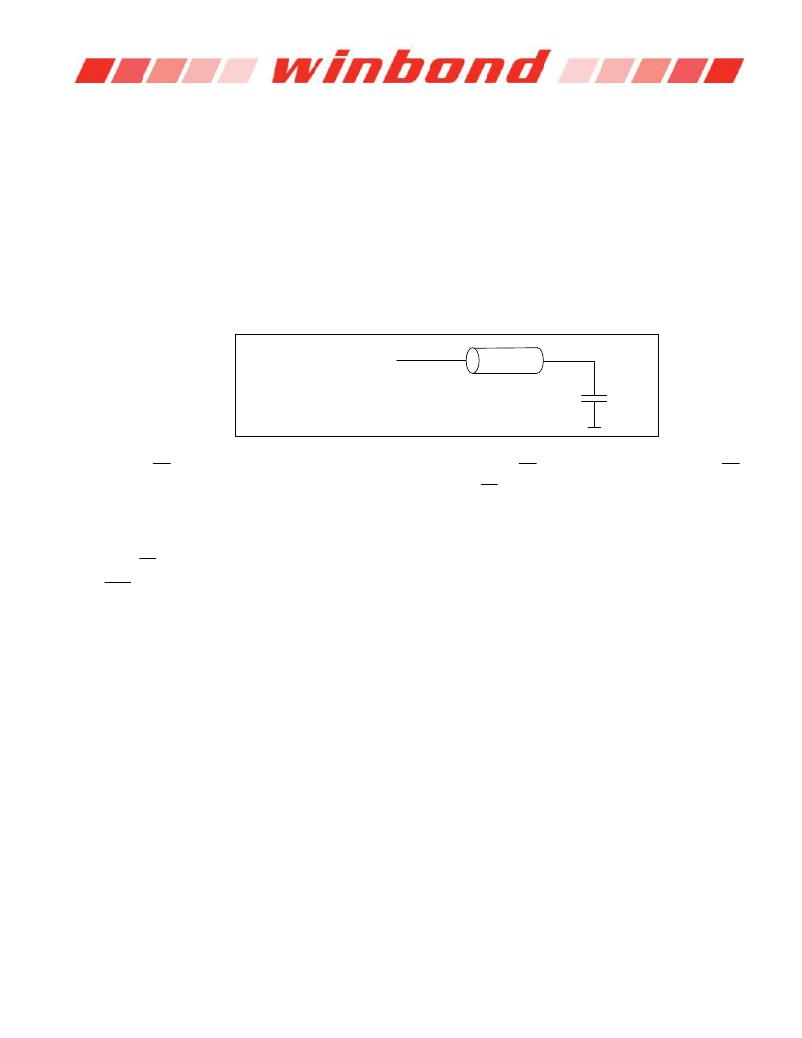
�The� circuit� shown� below� represents� the� timing� reference� load� used� in� defining� the� relevant� timing� parameters�
�of� the� part.� It� is� not� intended� to� be� either� a� precise� representation� of� the� typical� system� environment� nor� a�
�depiction� of� the� actual� load� presented� by� a� production� tester.� System� designers� will� use� IBIS� or� other�
�simulation� tools� to� correlate� the� timing� reference� load� to� system� environment.� Manufacturers� will� correlate� to�
�their� production� test� conditions� (generally� a� coaxial� transmission� line� terminated� at� the� tester� electronics).� For�
�the� half� strength� driver� with� a� nominal� 10pF� load� parameters� tAC� and� tQH� are� expected� to� be� in� the� same�
�range.� However,� these� parameters� are� not� subject� to� production� test� but� are� estimated� by� design� /�
�characterization.� Use� of� IBIS� or� other� simulation� tools� for� system� design� validation� is� suggested.�
�I/O�
�Time� Reference� Load�
�Z� 0� =� 50� Ohms�
�20pF�
�5.�
�6.�
�7.�
�8.�
�9.�
�10.�
�11.�
�12.�
�13.�
�14.�
�15.�
�16.�
�17.�
�18.�
�The� CK/� CK� input� reference� voltage� level� (for� timing� referenced� to� CK/� CK� )� is� the� point� at� which� CK� and� CK�
�cross;� the� input� reference� voltage� level� for� signals� other� than� CK/� CK� is� VDDQ/2.�
�The� timing� reference� voltage� level� is� VDDQ/2.�
�AC� and� DC� input� and� output� voltage� levels� are� defined� in� the� section� for� Electrical� Characteristics� and� AC/DC�
�operating� conditions.�
�A� CK/� CK� differential� slew� rate� of� 2.0� V/ns� is� assumed� for� all� parameters.�
�CAS� latency� definition:� with� CL� =� 3� the� first� data� element� is� valid� at� (2� *� tCK� +� tAC)� after� the� clock� at� which�
�the� READ� command� was� registered;� with� CL� =� 2� the� first� data� element� is� valid� at� (tCK� +� tAC)� after� the� clock� at�
�which� the� READ� command� was� registered�
�Min� (tCL,� tCH)� refers� to� the� smaller� of� the� actual� clock� low� time� and� the� actual� clock� high� time� as� provided� to�
�the� device� (i.e.� this� value� can� be� greater� than� the� minimum� specification� limits� of� tCL� and� tCH)�
�tQH� =� tHP� -� tQHS,� where� tHP� =� minimum� half� clock� period� for� any� given� cycle� and� is� defined� by� clock� high� or�
�clock� low� (tCL,� tCH).� tQHS� accounts� for� 1)� the� pulse� duration� distortion� of� on-chip� clock� circuits;� and� 2)� the�
�worst� case� push-out� of� DQS� on� one� transition� followed� by� the� worst� case� pull-in� of� DQ� on� the� next� transition,�
�both� of� which� are,� separately,� due� to� data� pin� skew� and� output� pattern� effects,� and� p-channel� to� n-channel�
�variation� of� the� output� drivers.�
�The� only� time� that� the� clock� frequency� is� allowed� to� change� is� during� clock� stop,� power-down� or� self-refresh�
�modes.�
�The� transition� time� for� DQ,� DM� and� DQS� inputs� is� measured� between� VIL(DC)� to� VIH(AC)� for� rising� input�
�signals,� and� VIH(DC)� to� VIL(AC)� for� falling� input� signals.�
�DQS,� DM� and� DQ� input� slew� rate� is� specified� to� prevent� double� clocking� of� data� and� preserve� setup� and� hold�
�times.� Signal� transitions� through� the� DC� region� must� be� monotonic.�
�Input� slew� rate� ≥� 1.0� V/ns.�
�Input� slew� rate� ≥� 0.5� V/ns� and� <� 1.0� V/ns.�
�These� parameters� guarantee� device� timing� but� they� are� not� necessarily� tested� on� each� device.�
�The� transition� time� for� address� and� command� inputs� is� measured� between� VIH� and� VIL.�
�Publication� Release� Date� :� Oct,� 15,� 2012�
�-� 53� -�
�Revision� :� A01-004�
�发布紧急采购,3分钟左右您将得到回复。
相关PDF资料
W949D2CBJX5E
IC LPDDR SDRAM 512MBIT 90VFBGA
W971GG6JB25I
IC DDR2 SDRAM 1GBIT 84WBGA
W971GG8JB-25
IC DDR2 SDRAM 1GBIT 60WBGA
W9725G6IB-25
IC DDR2-800 SDRAM 256MB 84-WBGA
W9725G6JB25I
IC DDR2 SDRAM 256MBIT 84WBGA
W9725G6KB-25I
IC DDR2 SDRAM 256MBIT 84WBGA
W972GG6JB-3I
IC DDR2 SDRAM 2GBITS 84WBGA
W9751G6IB-25
IC DDR2-800 SDRAM 512MB 84-WBGA
相关代理商/技术参数
W948D2FBJX5ETR
制造商:Winbond Electronics Corp 功能描述:256M MDDR, X32, 200MHZ
W948D2FBJX5I
制造商:Winbond Electronics Corp 功能描述:DRAM Chip DDR SDRAM 256M-Bit 8Mx32 1.8V 90-Pin VFBGA 制造商:Winbond Electronics Corp 功能描述:IC MEMORY
W948D2FBJX5I TR
制造商:Winbond Electronics Corp 功能描述:256M MDDR, X32, 200MHZ, INDUST
W948D2FBJX6E
制造商:Winbond Electronics Corp 功能描述:DRAM Chip DDR SDRAM 256M-Bit 8Mx32 1.8V 90-Pin VFBGA 制造商:Winbond Electronics 功能描述:LOW POWER DRAM 制造商:Winbond Electronics Corp 功能描述:IC MEMORY
W948D2FBJX6ETR
制造商:Winbond Electronics Corp 功能描述:256M MDDR, X32, 166MHZ, 65NM
W948D2FBJX6G
制造商:WINBOND 制造商全称:Winbond 功能描述:256Mb Mobile LPDDR
W948D6FB
制造商:WINBOND 制造商全称:Winbond 功能描述:256Mb Mobile LPDDR
W948D6FBHX5E
功能描述:IC LPDDR SDRAM 256MBIT 60VFBGA RoHS:是 类别:集成电路 (IC) >> 存储器 系列:- 标准包装:1 系列:- 格式 - 存储器:闪存 存储器类型:闪存 - NAND 存储容量:4G(256M x 16) 速度:- 接口:并联 电源电压:2.7 V ~ 3.6 V 工作温度:0°C ~ 70°C 封装/外壳:48-TFSOP(0.724",18.40mm 宽) 供应商设备封装:48-TSOP I 包装:Digi-Reel® 其它名称:557-1461-6